Revolutionizing PCB Design with SOLIDWORKS PCB Connector
Multidisciplinary engineering teams are working together more today than ever
before to develop products. This is because products now nee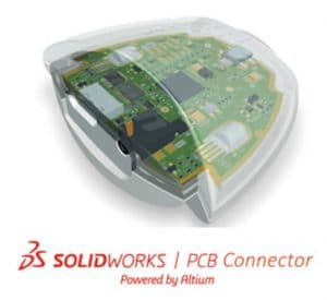 d to wirelessly connect and communicate with other devices, spurred by the rapid growth of the Internet of Things (IoT) within consumer electronics, manufacturing, healthcare, and automotive industries.
If you use Altium Designer, you can now maintain your preferred workflow and realize the value of the SOLIDWORKS PCB Connector, engineered specifically to bridge the gap between your electrical design in Altium and your mechanical design in SOLIDWORKS.
There are several advantages that both Printed Circuit Board (PCB) and SOLIDWORKS designers will notice given the ease of moving models back and forth between Altium Designer and SOLIDWORKS.
PCB Design Environment
Designers will be fully up and running on day one in their familiar Altium design environment. There are no changes to Altium Designer’s schematic and layout tools. Continue to work in Altium Designer and simply allow the SOLIDWORKS PCB Connector’s Project Collaboration Server to intelligently synchronize any changes made to your PCB design with your mechanical assembly in SOLIDWORKS.
Making changes to your PCB designs is not limited to your Altium Designer environment either. Changes can easily be made to component placement, board shape, and mounting holes directly in SOLIDWORKS, and automatically synced back to Altium Designer as an ECO. Mechanical designers find that being able to easily visualize component placement and height information based on 3D models solves many of their greatest concerns. Now, checking for interference and suggesting placement edits back to the PCB design environment couldn’t be easier.
Communication between PCB and Mechanical designers is essential. The PCB Connector allows users to include messages along with changes and track edits through time stamped dialogue history. This is especially useful during the initial design project, and is invaluable in the future if the design needs to be revisited by making change intent and timing clear.
Design Capabilities
The SOLIDWORKS PCB Connector makesit simple for the Mechanical designer to specify the board shape based on the model of the enclosure, or other mating part or assembly features. Since changes occur frequently during the design process, the ability to confirm fit within the enclosure right inside a SOLIDWORKS assembly is especially valuable.
Save time and effort by visually locating connectors and other components in 3D and easily moving them around and configuring dimensions based on the mechanical constraints. Even complex board shapes with curves and other traditionally hard to measure features and cutouts are easy to design using popular sketch tools right within SOLIDWORKS. This encourages innovation throughout the design process by the PCB and Mechanical designers.
Link directly to Parasolid models for enclosure and component bodies and then instantly view them in native 3D to ensure correct board fit within mechanical enclosures. Once your board is in the hands of the mechanical designer, a number of powerful simulation options await. Export board assemblies to SOLIDWORKS, with included copper information, to be used in detailed thermal, vibration, and mechanical simulationdata for the highest degree of design accuracy and reliability.
Time and Cost Savings
Data files are often shared ineffectively and unsafely using USB drives, emails, and loosely managed network drives. This wastes time and can result in costly data loss and confusion. The SOLIDWORKS PCB Connector ensures your data can be easily accessed and shared securely.
Prototypes are historically built to validate fit, but you can now accomplish the same results with fewer prototypes or no need for them at all. Save the significant time and cost associated with producing multiple prototypes and ensure your board fits right the first time.
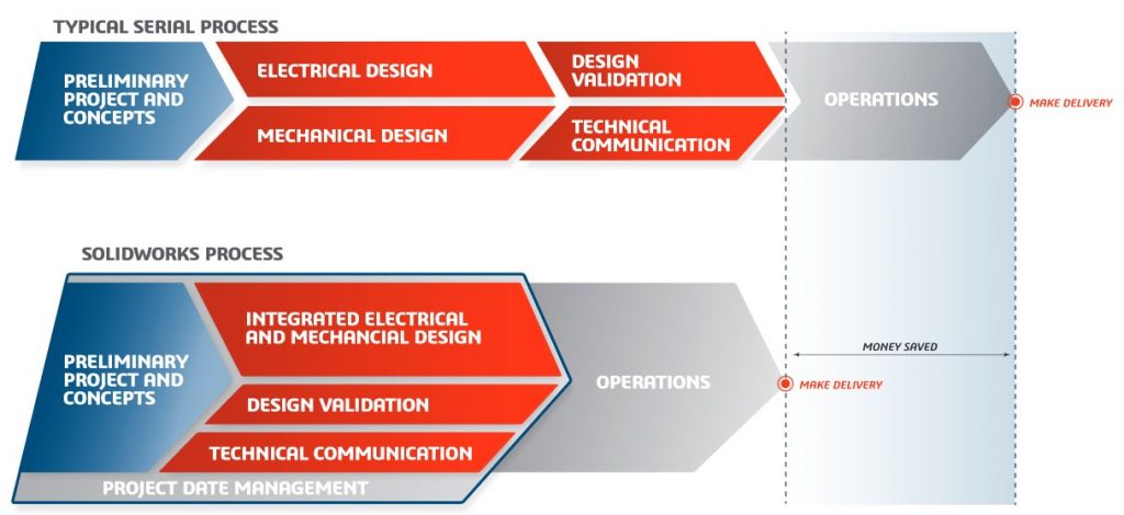
In today’s competitive landscape, design cycles must be improved in order to succeed. With the right tool, your company will be able to bring your product to market faster and more affordably by empowering your mechanical and electrical design teams to work concurrently.
It’s time to start investing in a new way for designers to become more productive and collaborate seamlessly – so they can focus more on designing and innovating – and experience less frustration with design changes, inefficient communication, data loss, and errors.
Retain and enhance the value of your Altium Designer investment with the SOLIDWORKS PCB Connector.