SOLIDWORKS PCB 2017 – ECAD to MCAD and Back – Printed Circuit Board Design
In SOLIDWORKS 2017 we introduce a new product in our line up called SOLIDWORKS PCB and PCB Connector. The development of printed circuit boards has been a part of the SOLIDWORKS design process on the mechanical side for quite some time now. However, we didn’t step into the actual development process of printed circuit board(PCB) schematics and layouts until now.
In this process, we begin to bridge the gap between ECAD and MCAD design. Instead of working in multiple design environments, we now work in only two. The PCB design environment and the SOLIDWORKS 3D CAD environment. By bridging these two environments we can develop a PCB with mechanical accuracy and work in a collaborative nature without worrying about how to exchange data.
SOLIDWORKS PCB is powered by Altium. In the figure below we can begin to see how a schematic can be developed with intelligence using simple tools:
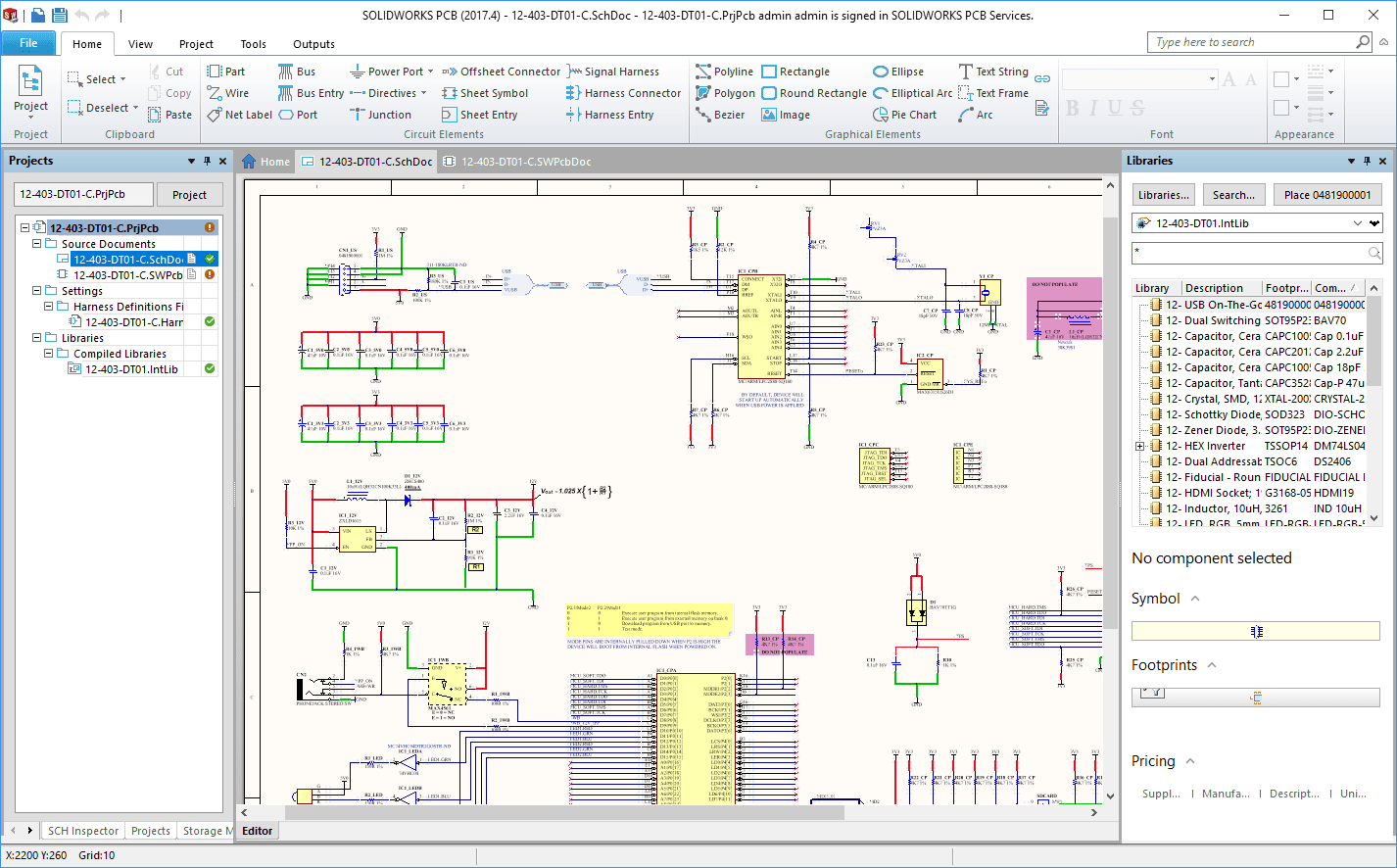
The schematic development side of a PCB has development tools and libraries to create component and connections while being organized and structured. Your schematic design will be directly tied to your PCB layout design as well:
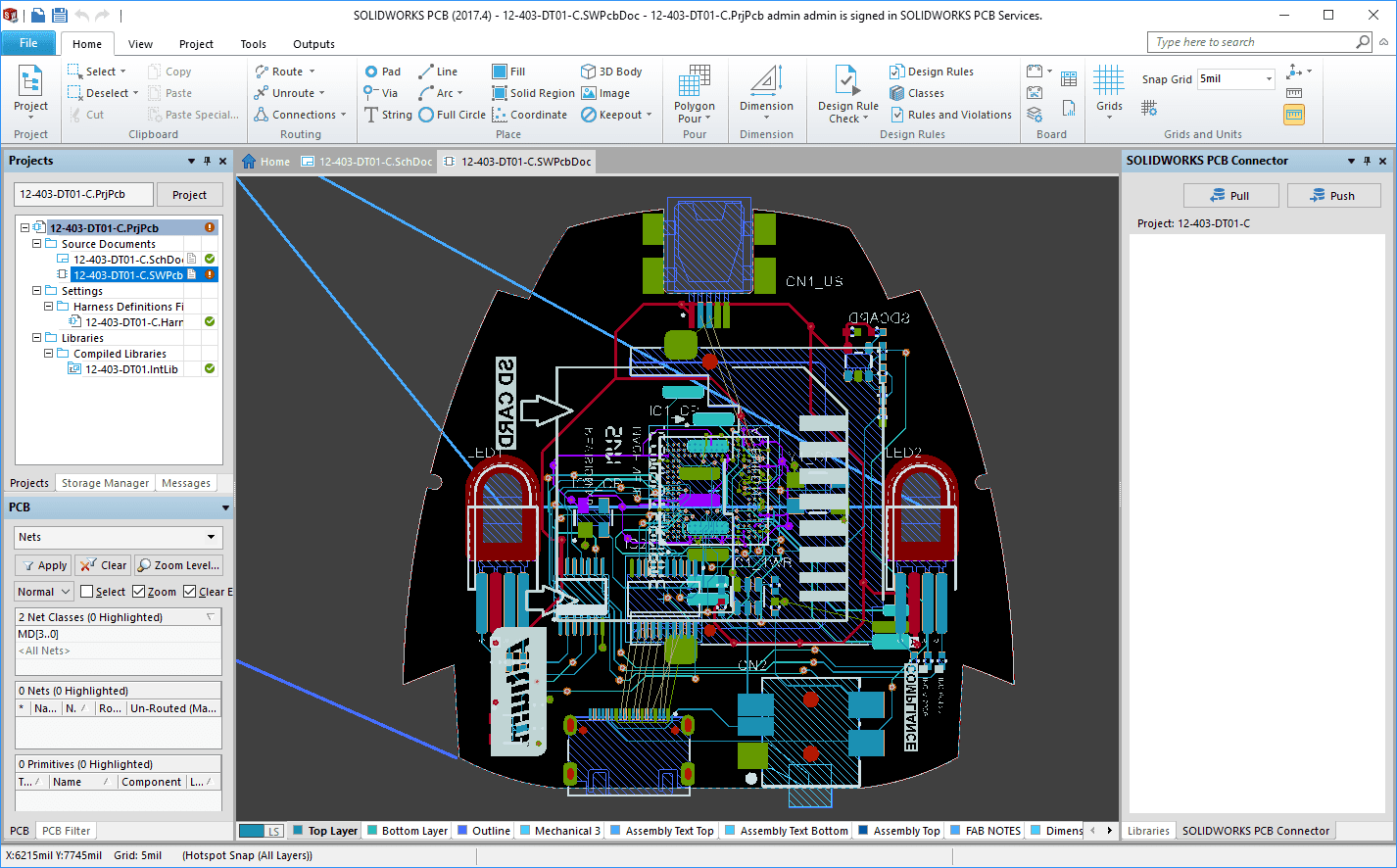
Just as we have tools to develop your schematic, we also have tools to create your layout design. Each component that we create in the schematic environment may have a footprint to use in the layout environment. Here we can begin to develop where our components will be as well as how we’ll develop the traces between the components.
Here’s where we have the ability to change how we develop the board itself. How do we shape the area of the board? How can we place components where we know there will not be interference to adjacent components or the enclosure? This is where developing the board in the mechanical environment becomes advantageous.
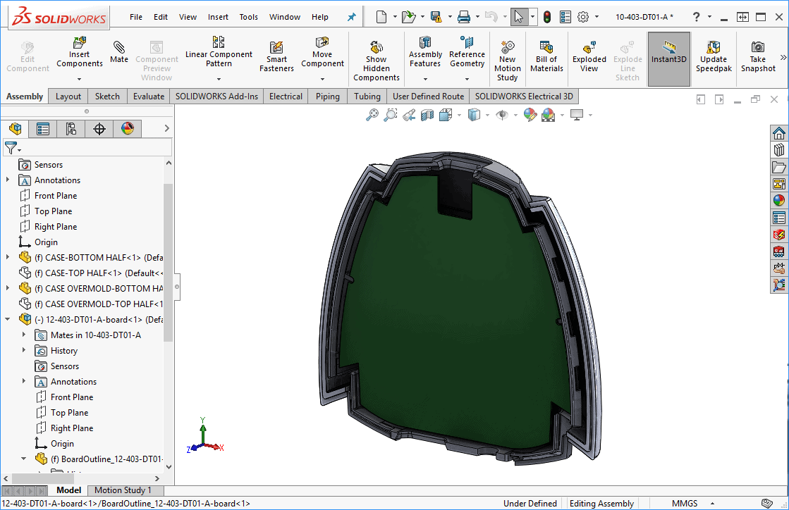
Within SOLIDWORKS PCB we have the ability to “Push” and “Pull” our designs an in easy collaborative system. When we have an initial board design, we can “Push” the board into the SOLIDWORKS environment:
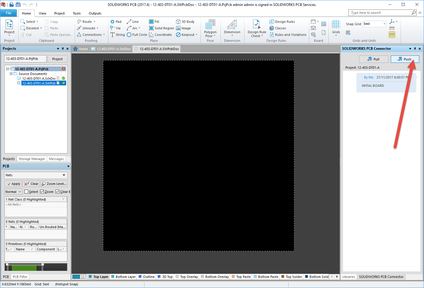
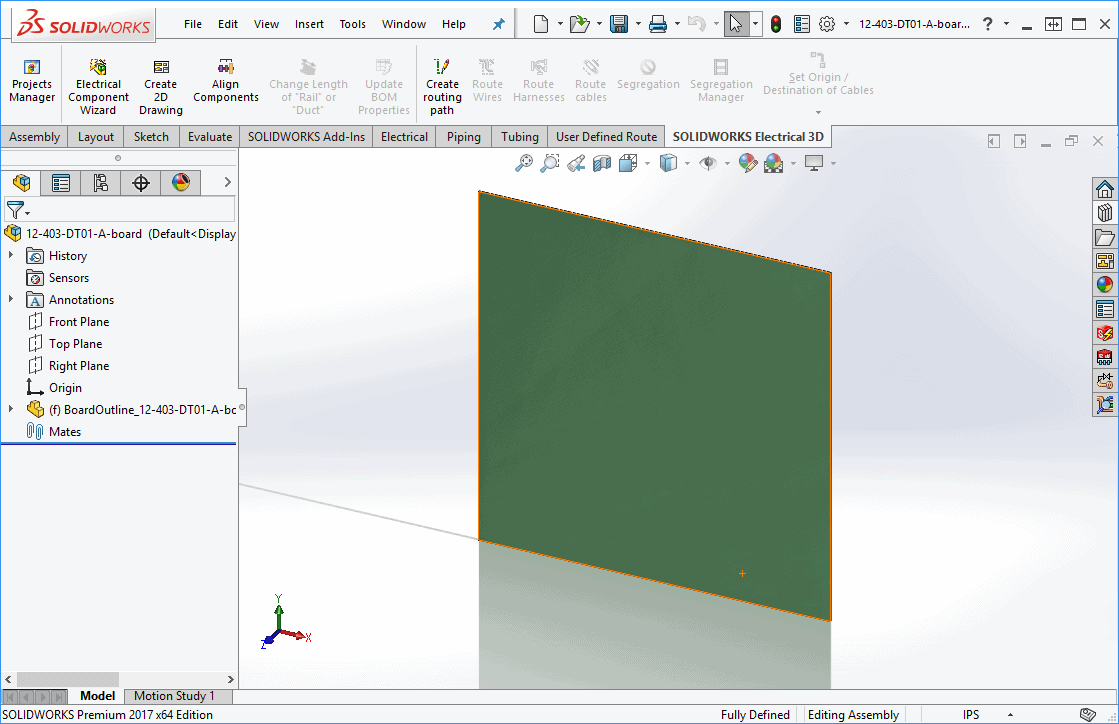
When we have the board in the SOLIDWORKS environment, we can shape the board, move components, move holes, check for interferences, and much more. With a change to the board shape, the changes are flagged in PCB layout and the changes can be immediately adapted into the design of the board.
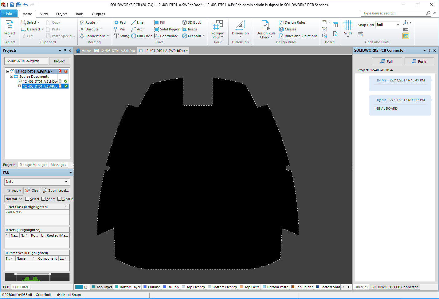
This exchange of data occurs quickly and allows our ECAD users to begin population of components and traces.
The collaboration ability in SOLIDWORKS PCB and PCB Connector (for current Altium users) allow our ECAD and MCAD teams to work together in a cohesive manner. With the SOLIDWORKS PCB we continue our efforts in developing a powerful development platform for designers in both the electronic and mechanical world.
Brian Do | Electrical Product Specialist
Computer Aided Technology (CATI)