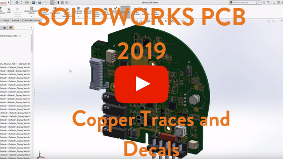
SOLIDWORKS PCB 2019: Copper Traces and Decals
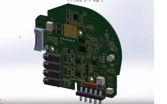 In SOLIDWORKS 2019, there are new capabilities for PCB collaboration to be able to import copper as well as decals into SOLIDWORKS. The control can be found in the setting for the collaboration and the first thing you’ll want to use is turn the option off for copper. In my example, I’ve pushed my design from SOLIDWORKS PCB 2019 with the copper option off and opened it inside of SOLIDWORKS Mechanical. In the image to the left, you can see that the decals and graphical representation of the top and bottom layer and there is no inner layer for copper in the design.
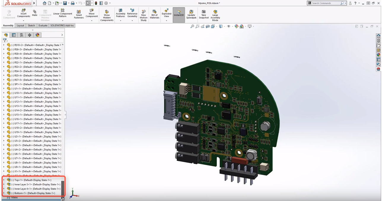
By turning the copper representation on, we’re going to reimport this design from SOLIDWORKS PCB. This new design will bring in additional information for decals and copper representation on all layers.
SOLIDWORKS Mechanical automatically notifies you of the new version from PCB noting that we have additional copper layer information. I’m going to accept these and open the design in SOLIDWORKS. The feature manager will now have additional layer information for the copper layer as well as decals from PCB.
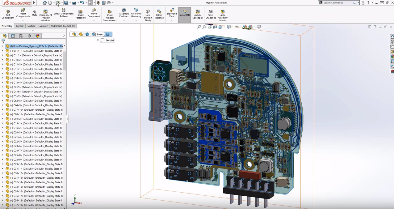
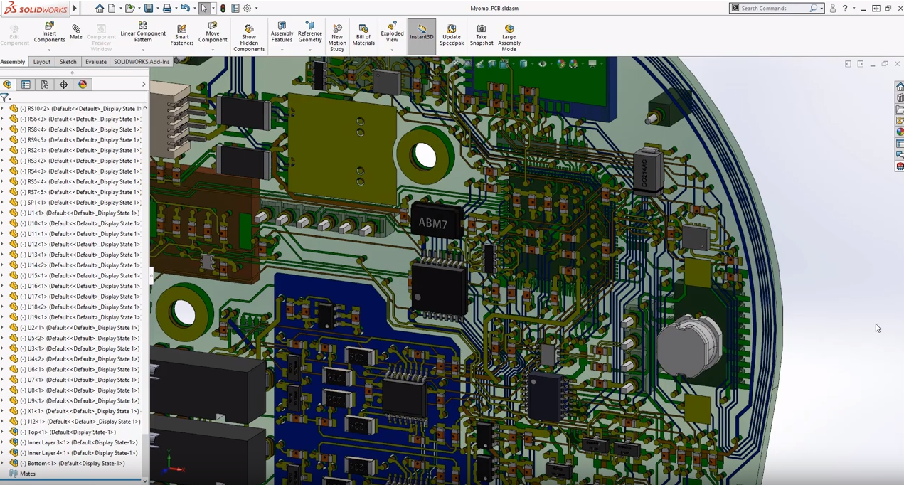
In SOLIDWORKS I’m going to change the transparency of the board so I can see inside the inner layers so now all the copper layers are visible inside of mCAD.
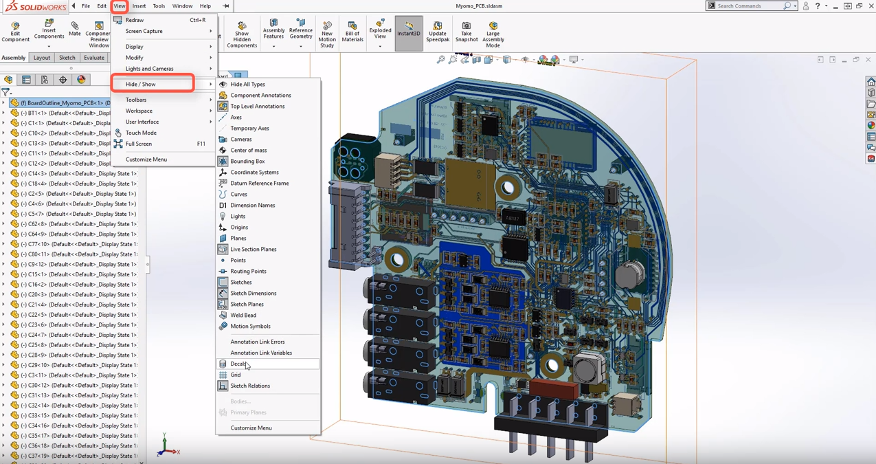
I’m then going to hide all of my decals so it’s easier to identify the inner layers.
I can assign different colors to the copper layers and you’ll see that every trace and every via can be viewed inside of SOLIDWORKS Mechanical just as it is in PCB. This allows my mechanical engineer to see how much copper is on each layer also allowing him to, later on, transfer this copper information into Flow Simulation for thermal analysis allowing PCB to collaborate with my mCAD for in-depth studies.
When we design PCB boards, we don’t always know the location of mounting holes for other mechanical features. Using SOLIDWORKS PCB collaboration, I’m going to send a blank board to my mechanical engineer and have him add mounting holes in SOLIDWORKS.
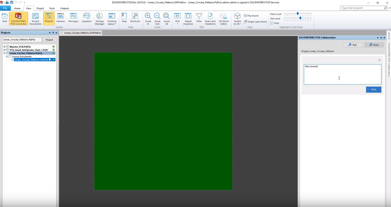
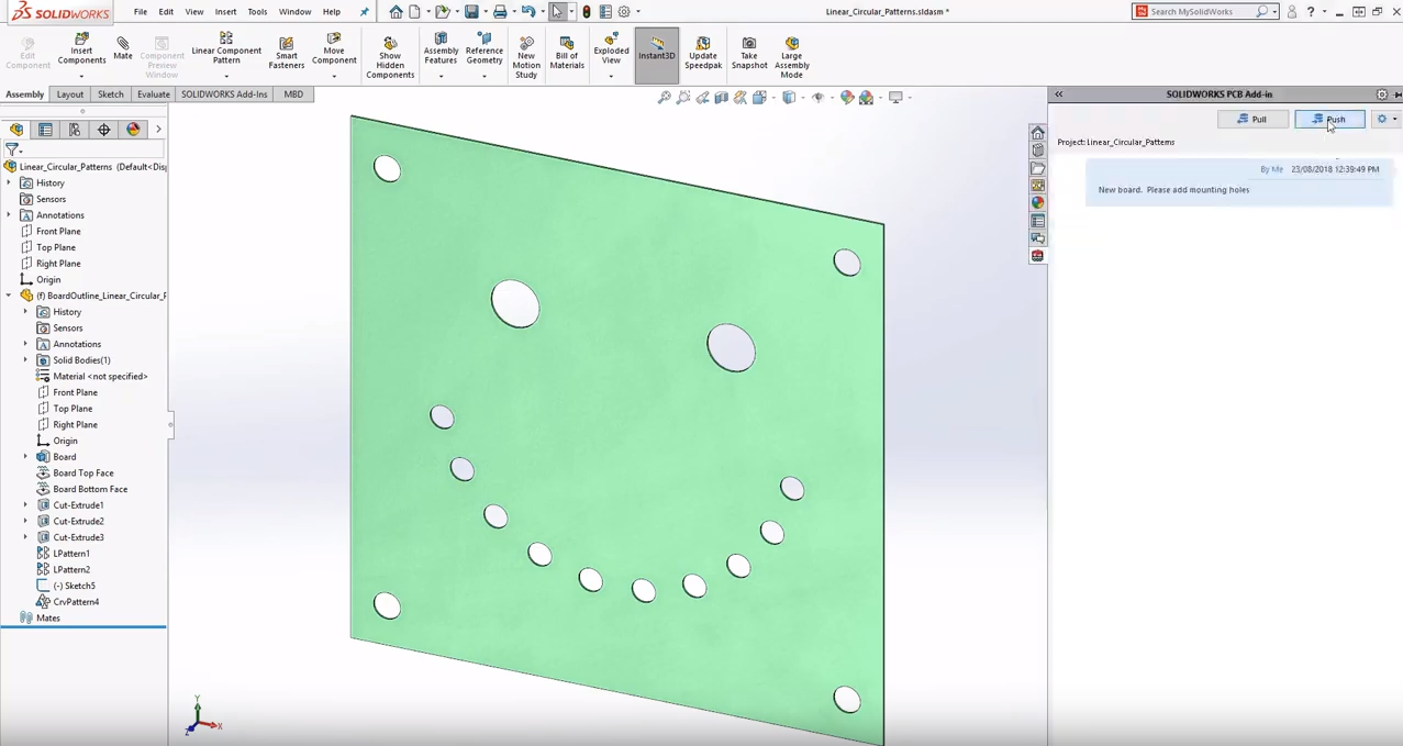
Using the same SOLIDWORKS PCB collaboration, we’re going to look for a blank board that we have sent by searching in projects and opening in SOLIDWORKS. The mechanical engineer has added different size holes in the board utilizing many of the SOLIDWORKS patterning features to create them. Once he has completed his design, he’ll push it back to SOLIDWORKS PCB.
SOLIDWORKS PCB 2019 automatically notifies you when a mechanical engineer has made changes.
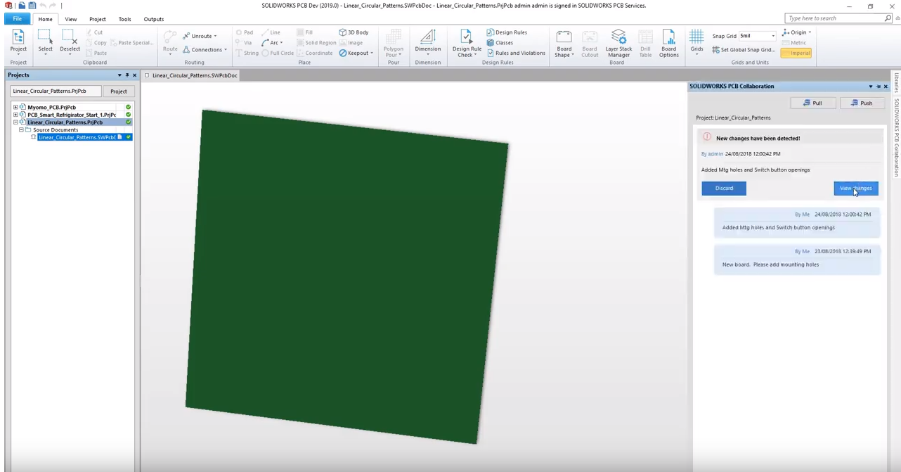
We’re accepting all the mounting and other holes which will automatically show up in PCB. This is a tremendous time saver to leverage SOLIDWORKS Mechanical capabilities by adding holes of different style patterns and effortlessly incorporating them into SOLIDWORKS PCB eliminating any possible misalignment between mCAD and eCAD.
Related Articles
The Best of SOLIDWORKS 2019 (Part 1)
The Best of SOLIDWORKS 2019 (Part 2)
About the Author
 Angelle Erickson writes about how companies are using innovative technologies, such as 3D printers and SOLIDWORKS software to increase productivity, improve product development processes, and maximize business potential.