The Makings of a Readable PCB Schematic
We draw a schematic to define the connections that are going to be made on the PCB layout, and so we sometimes get lost in that purpose, forgetting that when everything is done there are good odds that someone else is going to have to reference what we’ve drawn and decipher it. We understand it, and it works well enough to get the netlist created for the routing, but can someone else look at it to do troubleshooting or understand the functional intent of the design? It’s important that we follow conventions that will ensure clear communication.
Take for instance this circuit:
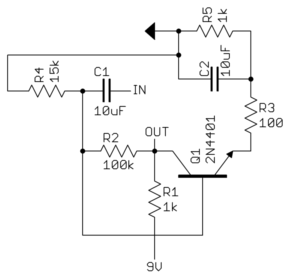
It works. The netlist is created and I can route it on a PCB. But if you wanted to figure out what it was, you’d have to do some deciphering. Here’s the same circuit, drawn in a more conventional manner:
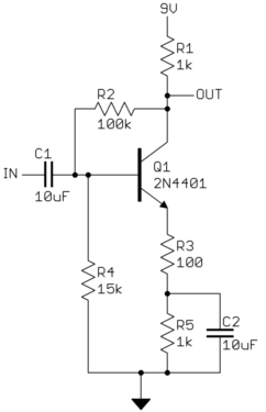
One look and you’ll realize it’s a common emitter amplifier.
So what are some common rules for a schematic design that we should all follow? If you are just starting to get into designing circuit boards to jump on the IOT craze, then you may not know/remember all of these.
Schematics should read left to right, top to bottom
It should read like a book. Inputs go on the left, outputs on the right, and the signal flows left to right. If you reach the end of the page and need to go to a new row, don’t make the next row flow right to left. Bring the wires from the first row all the way back to the left side of the page to start a new row. If you don’t like how that looks, then use ports or net name to tie the netlist together without the visual of the long wire.
Clean up the text around your symbols
Sometimes the schematic gets crowded and we end up with a lot of text in a small area. Make sure all of the text is oriented the same way, you can easily tell which symbol for which it is providing information, and you don’t have wires or symbol lines running through the text. How easy is this to read?
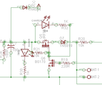
Answer: not very.
Name your nets, and group related signals together
SOLIDWORKS PCB will name your nets for you if you don’t apply your own names, so that it can generate a netlist, but you won’t see those names except when routing. However, if you give them your own (meaningful) names, it will be a lot easier to understand your design intent. Here is a page of ANSI/IEEE recommended net name abbreviations.
Also, we have the ability to group related signals together into a bus or signal harness. This will keep you from having to route multiple wires alongside each other to their destination, taking up valuable real estate. In the image below you can see how you can utilize a bus. Imagine how many wires you would have crossing over each other if I represented them all individually. We know which wire goes from which origin to which destination based on the matching net names.
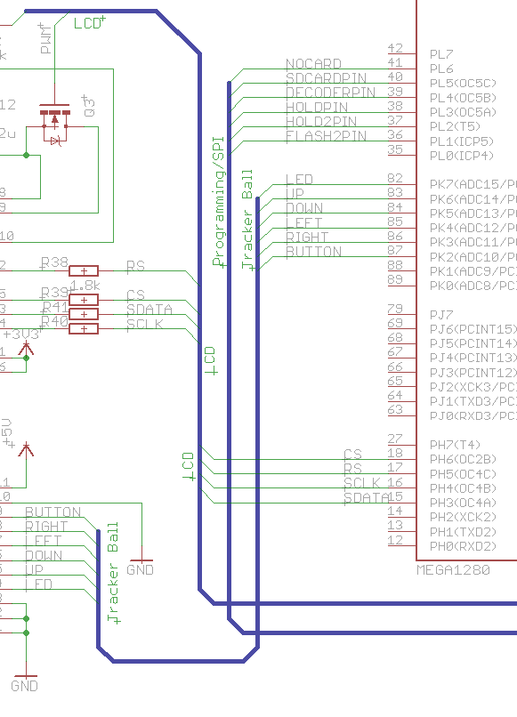
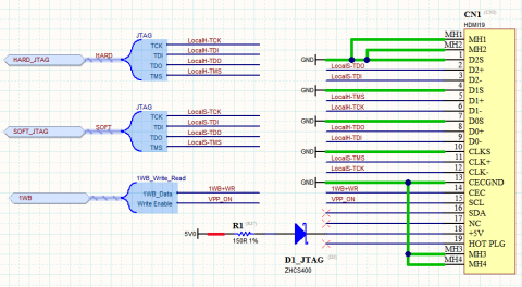
Here you can see how SOLIDWORKS PCB uses signal harnesses to group wires together into a single port so that you can easily connect multiple wires across different pages. You’ll notice that we don’t have a lot of wires crossing over themselves either, utilizing just the net names to show connection. It is more readable than trying to follow a lot of criss-crossing wires, but if you make your entire schematic using “air” wires it can become just as illegible. I’ll leave that one up to you to decide which you want to follow.
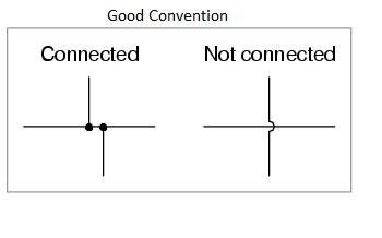
Don’t connect wires using a 4-way tie
When it comes to wires crossing other wires on a schematic, you don’t want to leave your reader guessing what you mean. Some people will have two lines crossing each other, meaning that they are connected, others assume not connected. Using a bridge or connection dot certainly makes it more clear.
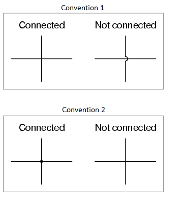
I would argue that to make it the most clear, never cross wires without a bridge, and never cross wires where you mean them to be connected. Offset one of the wires a little bit so that they won’t be wondering if you use connection dots or not. Both ways of showing wires in convention 2 above, are bad.
Decoupling Capacitor Placement
Locate decoupling capacitors close to the components they serve. I have seen schematics where they are all located on a single page by themselves. This doesn’t communicate to the layout engineer their purpose and where they should place it. Also, if the plan is to reuse circuitry in the future, across multiple designs, then keeping the decoupling caps close to the components they filter will make it quicker and easier to create reusable design blocks.
Design for regular size paper
No one is sitting around with drafting tables to look at D-size paper anymore. Most people only have access to printers that will print on 8 1/2 x 11 inch or 11 x 17 inch paper. Don’t use a size D title block so that you can cram a bunch of symbols on a single page. It will just get printed on a smaller page and end up needing a magnifying glass to read. Also, if someone is looking at it on a computer screen they will have to pan around a lot to follow. If using a smaller title block means more pages, go ahead. You can flip pages back and forth with a single click in Adobe Reader. Flipping pages is preferable to constantly panning, zooming out and in. Think of pages in schematics like paragraphs in a narrative. Breaking a schematic into individually labeled sections by pages can help readability if done right. For example, you might have a page for the power input section, the immediate microcontroller connections, the analog inputs, the H bridge drive power outputs, the ethernet interface, etc. It’s actually useful to break up the schematic this way even if it had nothing to do with drawing size.