SOLIDWORKS 2017 What's New: SOLIDWORKS PCB – #SW2017
SOLIDWORKS PCB
In SOLIDWORKS 2017 there are several new features and products entering into the SOLIDWORKS product environment. With electro-mechanical design, we often see a disconnect between electrical and mechanical designers. To bridge this gap, we have added innovative tools to unify design under the SOLIDWOKS umbrella. With the release of SOLIDWORKS 2016 SP3.0, we are proud to introduce a new product for the design of printed circuit boards called SOLIDWORKS PCB.
SOLIDWORKS PCB was added into the product line to help electronics and mechanical designers collaborate during the development of printed circuit boards. This tool allows and introduces a new workflow for the design of PCBs.
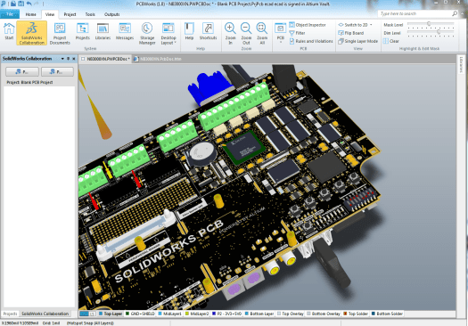
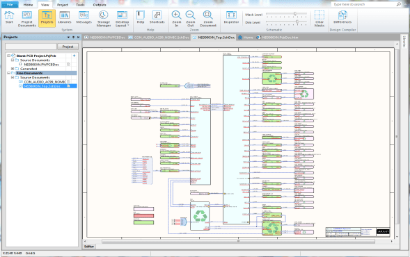
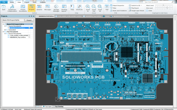
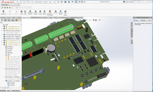
Internally, SOLIDWORKS PCB has the backbone of Altium with the user interface that is similar to the SOLIDWORKS environment. This means we’re using 30+ years of Altium’s PCB experience right in our software. When we consider the workflow for design, we’re looking at three main areas: schematic capture, PCB layouts, and mechanical integration. SOLIDWORKS PCB unifies all three areas.
Now, how do we do this? How do we develop it in software?
If we were to start in a standard design workflow, we can begin with first creating our design schematic. SOLIDWORKS PCB allows us to find components from an enormous online database of parts. These parts are available from real-time component supplier links, which decreases the amount of time needed to find suitable parts for your design. From here we translate the schematic information to layout information with both 2D footprint information and 3D visual information.
Between these two design areas, you never leave the interface of SOLIDWORKS PCB. But now, how do we then translate our design information for the mechanical designers? Often times we need to make sure that our PCB can fit into different enclosures. The mechanical integration from SOLIDWORKS PCB to the mechanical SOLIDWORKS environment is done with a very simple push/pull system. Whenever either design needs to make a change to the board, they can simply ‘push’ their design to each other’s environment.
For example, let’s say that our electronics designer has completed 20% of their design and would like to shape the board and add mounting holes. They can ‘push’ their design into the SOLIDWORKS environment where the mechanical designer can shape the board directly in their assembly and constrain the locations of the mounting hole to exactly where they need to board to fit.
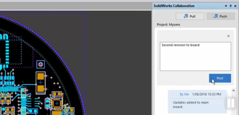
From there the changes made by the mechanical designer can be pushed back to SOLIDWORKS PCB without ever worrying about export/import information.
SOLIDWORKS PCB has many powerful tools for electronics design and its collaborative nature brings unity into the SOLIDWORKS environment.
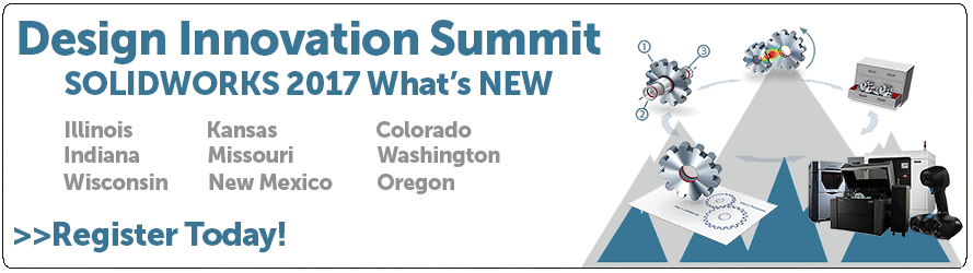
I hope this part of the What’s New series gives you a better understanding of the new features and functions of SOLIDWORKS 2017. Please check back to the CATI Blog as the CATI and MCAD Support Teams will continue to break down many of the new items in SOLIDWORKS 2017. All of these articles will be stored in the category of “SOLIDWORKS What’s New.” You can also learn more about SOLIDWORKS 2017 by clicking on the image below to register for one of CATI’s or CATI’s Design Summits.
Brian Do
Applications Engineer, Electrical
Computer Aided Technology